- 您现在的位置:买卖IC网 > Sheet目录369 > W948D2FBJX5E (Winbond Electronics)IC LPDDR SDRAM 256MBIT 90VFBGA
�� �
�
�W948D6FB� /� W948D2FB�
�256Mb� Mobile� LPDDR�
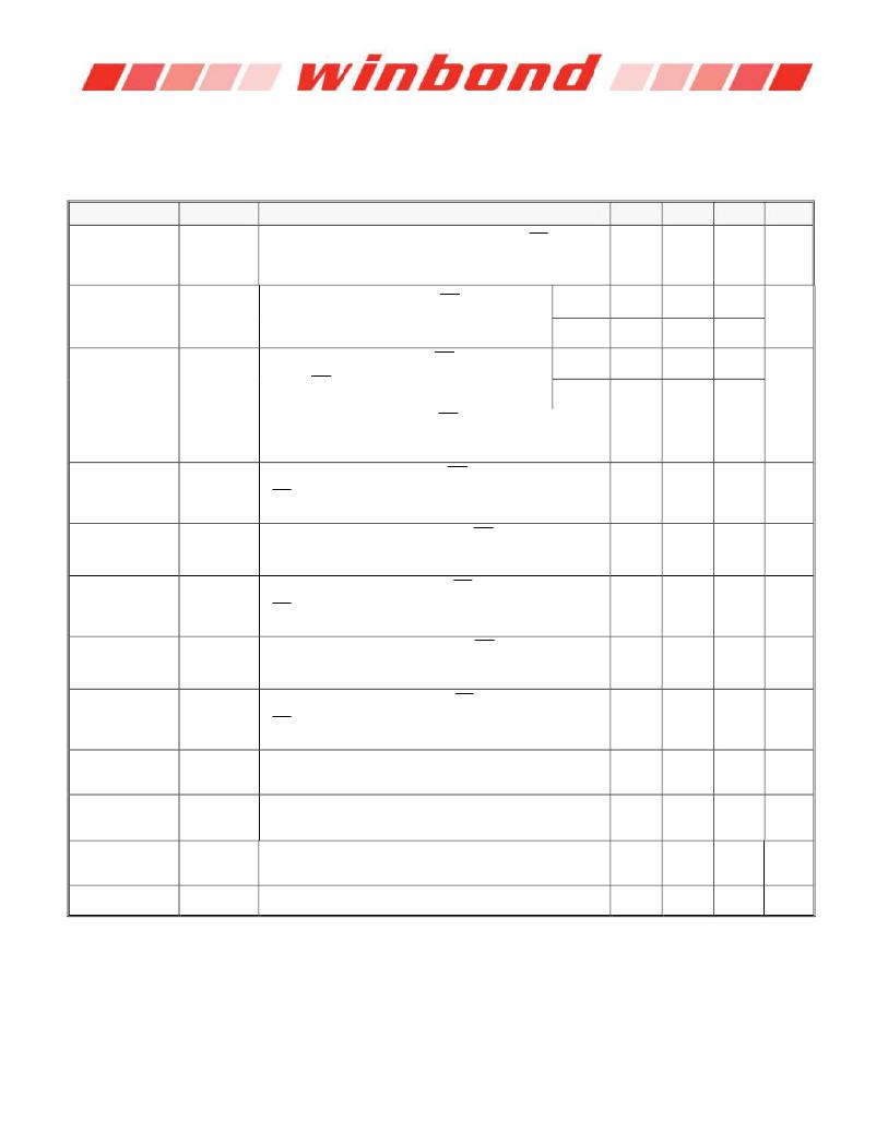
�8.4� IDD� Specification� Parameters� and� Test� Conditions�
�8.4.1� IDD� Specification� Parameters� and� Test� Conditions�
�[Recommended� Operating� Conditions;� Notes� 1-3]�
�(256Mb,� X16)�
�PARAMETER�
�Operating� one�
�bank� active-�
�precharge�
�current�
�SYMBOL�
�IDD0�
�TEST� CONDITION�
�tRC� =� tRCmin� ;� tCK� =� tCKmin� ;� CKE� is� HIGH;� CS� is� HIGH�
�between� valid� commands;� address� inputs� are�
�SWITCHING;� data� bus� inputs� are� STABLE�
�-5�
�40�
�-6�
�38�
�-� 75�
�35�
�UNIT�
�mA�
�Precharge�
�power-down�
�standby� current�
�Precharge�
�power-down�
�standby� current�
�with� clock� stop�
�IDD2P�
�IDD2PS�
�all� banks� idle,� CKE� is� LOW;� CS� is� HIGH,� tCK�
�=� tCKmin� ;� address� and� control� inputs� are�
�SWITCHING;� data� bus� inputs� are� STABLE�
�all� banks� idle,� CKE� is� LOW;� CS� is� HIGH,� CK� =�
�LOW,� CK� =� HIGH;� address� and� control� inputs�
�are� SWITCHING;� data� bus� inputs� are� STABLE�
�Low�
�power�
�Normal�
�power�
�Low�
�power�
�Normal�
�power�
�0.3�
�0.4�
�0.3�
�0.4�
�0.3�
�0.4�
�0.3�
�0.4�
�0.3�
�0.4�
�0.3�
�0.4�
�mA�
�mA�
�Precharge� non�
�power-down�
�standby� current�
�Precharge� non�
�power-down�
�standby� current�
�IDD2N�
�IDD2NS�
�all� banks� idle,� CKE� is� HIGH;� CS� is� HIGH,� tCK� =� tCKmin;�
�address� and� control� inputs� are� SWITCHING;� data� bus�
�inputs� are� STABLE�
�all� banks� idle,� CKE� is� HIGH;� CS� is� HIGH,� CK� =� LOW,�
�CK� =� HIGH;� address� and� control� inputs� are�
�10�
�3�
�10�
�3�
�10�
�3�
�mA�
�mA�
�with� clock� stop�
�SWITCHING;� data� bus� inputs� are� STABLE�
�Active� power-�
�down� standby�
�current�
�Active� power-�
�down� standby�
�current� with�
�IDD3P�
�IDD3PS�
�one� bank� active,� CKE� is� LOW;� CS� is� HIGH,� tCK� =�
�tCKmin;address� and� control� inputs� are� SWITCHING;� data�
�bus� inputs� are� STABLE�
�one� bank� active,� CKE� is� LOW;� CS� is� HIGH,� CK� =� LOW,�
�CK� =� HIGH;� address� and� control� inputs� are�
�3�
�3�
�3�
�3�
�3�
�3�
�mA�
�mA�
�clock� stop�
�SWITCHING;� data� bus� inputs� are� STABLE�
�Active� non�
�power-down�
�standby� current�
�Active� non�
�power-down�
�standby� current�
�IDD3N�
�IDD3NS�
�one� bank� active,� CKE� is� HIGH;� CS� is� HIGH,� tCK� =�
�tCKmin;� address� and� control� inputs� are� SWITCHING;� data�
�bus� inputs� are� STABLE�
�one� bank� active,� CKE� is� HIGH;� CS� is� HIGH,� CK� =� LOW,�
�CK� =� HIGH;� address� and� control� inputs� are�
�25�
�15�
�20�
�12�
�20�
�12�
�mA�
�mA�
�with� clock� stop�
�SWITCHING;� data� bus� inputs� are� STABLE�
�Operating� burst�
�read� current�
�Operating� burst�
�write� current�
�Auto-Refresh�
�Current�
�Deep� Power-�
�Down� current�
�IDD4R�
�IDD4W�
�IDD5�
�IDD8(4)�
�one� bank� active;� BL� =� 4;� CL� =� 3;� tCK� =� tCKmin� ;�
�continuous� read� bursts;� IOUT� =� 0� mA;� address� inputs� are�
�SWITCHING;� 50%� data� change� each� burst� transfer�
�one� bank� active;� BL� =� 4;� tCK� =� tCKmin� ;� continuous� write�
�bursts;� address� inputs� are� SWITCHING;� 50%� data� change�
�each� burst� transfer�
�tRC� =� tRFCmin� ;� tCK� =� tCKmin� ;� burst� refresh;� CKE� is�
�HIGH;� address� and� control� inputs� are� SWITCHING;� data�
�bus� inputs� are� STABLE�
�Address� and� control� inputs� are� STABLE;� data� bus� inputs�
�are� STABLE�
�75�
�55�
�50�
�10�
�70�
�50�
�50�
�10�
�70�
�50�
�50�
�10�
�mA�
�mA�
�mA�
�uA�
�Publication� Release� Date� :� Oct,� 15,� 2012�
�-� 48� -�
�Revision� :� A01-004�
�发布紧急采购,3分钟左右您将得到回复。
相关PDF资料
W949D2CBJX5E
IC LPDDR SDRAM 512MBIT 90VFBGA
W971GG6JB25I
IC DDR2 SDRAM 1GBIT 84WBGA
W971GG8JB-25
IC DDR2 SDRAM 1GBIT 60WBGA
W9725G6IB-25
IC DDR2-800 SDRAM 256MB 84-WBGA
W9725G6JB25I
IC DDR2 SDRAM 256MBIT 84WBGA
W9725G6KB-25I
IC DDR2 SDRAM 256MBIT 84WBGA
W972GG6JB-3I
IC DDR2 SDRAM 2GBITS 84WBGA
W9751G6IB-25
IC DDR2-800 SDRAM 512MB 84-WBGA
相关代理商/技术参数
W948D2FBJX5ETR
制造商:Winbond Electronics Corp 功能描述:256M MDDR, X32, 200MHZ
W948D2FBJX5I
制造商:Winbond Electronics Corp 功能描述:DRAM Chip DDR SDRAM 256M-Bit 8Mx32 1.8V 90-Pin VFBGA 制造商:Winbond Electronics Corp 功能描述:IC MEMORY
W948D2FBJX5I TR
制造商:Winbond Electronics Corp 功能描述:256M MDDR, X32, 200MHZ, INDUST
W948D2FBJX6E
制造商:Winbond Electronics Corp 功能描述:DRAM Chip DDR SDRAM 256M-Bit 8Mx32 1.8V 90-Pin VFBGA 制造商:Winbond Electronics 功能描述:LOW POWER DRAM 制造商:Winbond Electronics Corp 功能描述:IC MEMORY
W948D2FBJX6ETR
制造商:Winbond Electronics Corp 功能描述:256M MDDR, X32, 166MHZ, 65NM
W948D2FBJX6G
制造商:WINBOND 制造商全称:Winbond 功能描述:256Mb Mobile LPDDR
W948D6FB
制造商:WINBOND 制造商全称:Winbond 功能描述:256Mb Mobile LPDDR
W948D6FBHX5E
功能描述:IC LPDDR SDRAM 256MBIT 60VFBGA RoHS:是 类别:集成电路 (IC) >> 存储器 系列:- 标准包装:1 系列:- 格式 - 存储器:闪存 存储器类型:闪存 - NAND 存储容量:4G(256M x 16) 速度:- 接口:并联 电源电压:2.7 V ~ 3.6 V 工作温度:0°C ~ 70°C 封装/外壳:48-TFSOP(0.724",18.40mm 宽) 供应商设备封装:48-TSOP I 包装:Digi-Reel® 其它名称:557-1461-6